Lip-Bu Tan, chief executive of Intel, this week confirmed that the company had already begun to work on its 10A and 7A fabrication technologies that will succeed Intel's current-generation 18A and next-generation 14A production nodes sometime in the next decade. Both 10A and 7A processes will presumably be able to use ASML's EUV lithography tools with high numerical aperture optics (High-NA), which will first be used for 14A.
"Now I am starting to work 10A, 7A, the roadmap," said Lip-Bu Tan at JP Morgan's Global Technology, Media and Communications Conference. "People do not [simply] go to you, they are looking for the roadmap for the future. So we want to build a long-term business. […]."
Tan emphasized a long-known business practice that ambitious roadmaps that are properly executed are as important as competitive products or fabrication technologies, as many companies do not just buy products, but roadmaps, as they prefer to work with suppliers for years to come. That said, Intel must offer its partners long-term roadmap visibility, so it has to work on technologies that are years from commercialization.
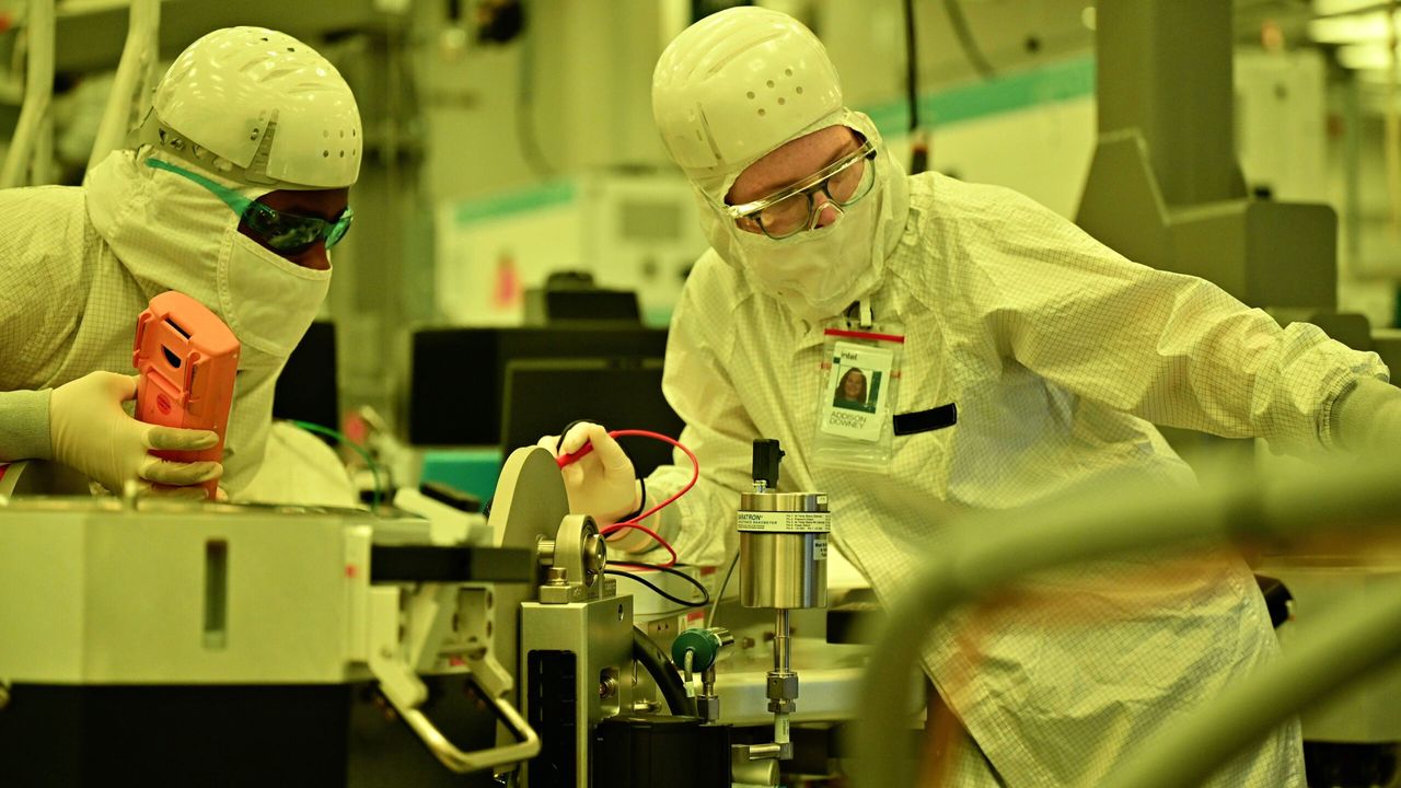
When it comes to Intel's 14A, its development is proceeding as planned, with version 0.5 of the process design kit (PDK) already available and version 0.9 of the PDK due in October.
"Clearly, the 14A, and we announced in Q1, we have v0.5 PDK so that they can do the test chip to look at our yield and see whether they can, over time, to really design their product and fabricate with us," Tan said. "The Holy Grail is v0.9 PDK. Right now, we are looking at October to [hand it to] the outside customer. Internal customer will be earlier, so that we make sure that we really clean the pipe, make sure that we are doing right, make sure that we can sell with good quality."
Tan says multiple customers have expressed interest in 14A, though Intel has not yet disclosed them.
"We have multiple customers engaged with us [with 14A], and to really define what product, what foundry location wants to be, what kind of capacity we need," Tan said. "I do not disclose the customer. If the customer wants to disclose, we will support that."
As for Intel's 14A timeline, Intel expects risk production in 2028 and then volume production in 2029, which is about the time when TSMC begins to volume produce chips on its A14 fabrication technology.
Three things must be kept in mind here. Firstly, TSMC's A14 is not a direct rival for Intel's 14A as the latter features backside power delivery and is better suitable for high-end data center-grade processors. Secondly, TSMC is said to start making chips using A14 in late 2028, and the company tends to initiate high volume manufacturing (HVM) with very high yields and volumes. By contrast, Intel initiates volume production at development fabs, and it takes the company some time to reach comparable yields and volumes. Thirdly, Intel's 14A will be one of the first nodes to be compatible with High-NA EUV lithography systems (for select layers) and will be the first production node to have the capability to use such scanners for high-volume manufacturing.
Insertion of all-new High-NA EUV tools — along with new photoresists, new photomasks, new pellicles, new metrology tools, new design rules, new computational lithography flows, and a lot of other innovations — is not going to be easy for Intel, so the company is hard at work working with both ASML and partners to ensure that the new ecosystem is ready for prime time. Coincidentally, Christophe Fouquet, the head of ASML, reportedly said that the first test chips made using these High-NA EUV tools will emerge in the coming months, though he did not specify at which vendor or facility.